
Result
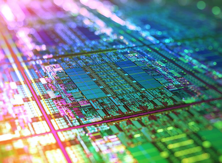
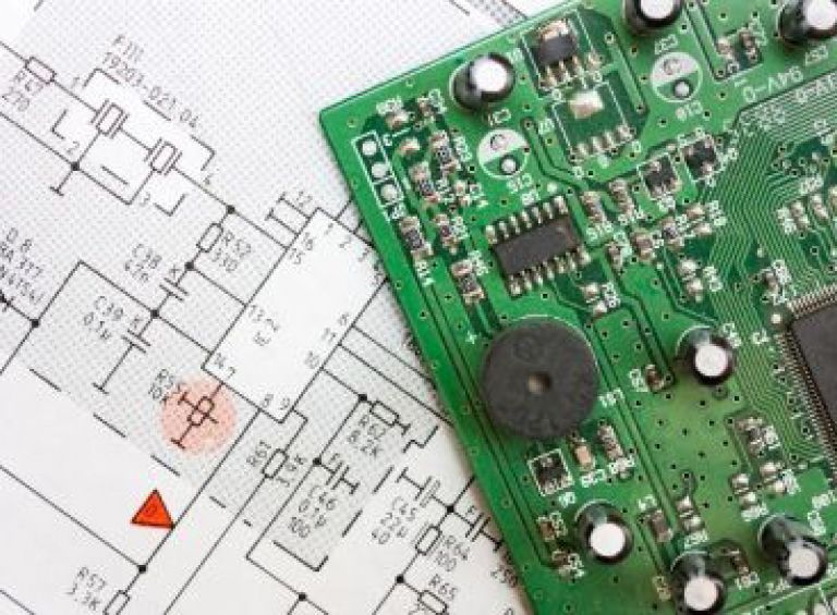
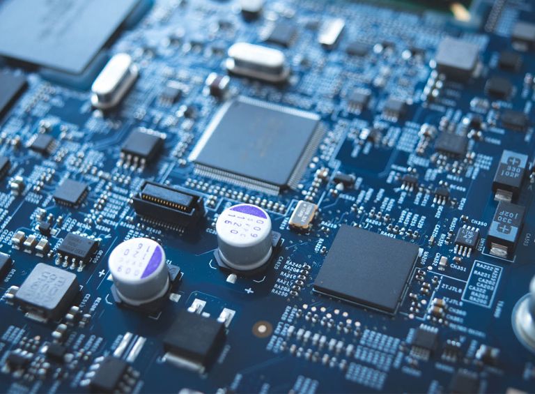
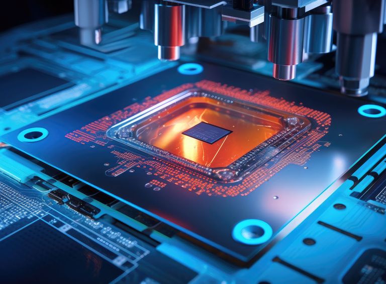
Industries such as Military-Aerospace, Medical, Telecom, and Industrial Electronics rely on fine-pitch packages (QFPs and BGAs) and increased package pin counts to support their interconnect designs. To meet these demands, High-Density Interconnect (HDI) and Ultra High-Density Interconnect (UHDI) technologies play a critical role. When properly integrated into the PCB structure, HDI improves both signal integrity and via reliability.
The success or failure of product performance, reliability, and time to market is heavily influenced by the materials, processes, and designs of these enabling technologies. To equip professionals with the necessary skills and process knowledge, IPC developed this course.

Advanced Packaging: Introduction to Polymers introduces the types of polymers and polymer composites used in advanced packaging applications, package types, and trends in packaging architecture.
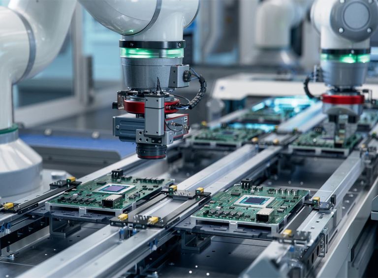
In this course, we will review the data produced by factory machines such as SMT and test equipment and how AI tools can be leveraged to assist with the analysis and interpretation of the data. The course is designed around practical, interactive learning experiences with an anonymized real-world dataset and freely available analysis and visualization tools. AI agents and copilots will be directly created live in the course using UI tools to visually illustrate the concepts and show what is possible with current technologies.

It’s more than a credential; it’s your proof of professional readiness. As a Certified Altium Designer Associate, you demonstrate the technical competence and design discipline employers expect from skilled PCB design engineers. Whether you’re looking to build credibility in your first role or strengthen your standing on a design team, Altium certification sets you apart in a competitive field.
The Certified Advanced Altium Designer is a subject matter professional with advanced knowledge and understanding of Altium Designer software. This certification exam will focus on complex concepts and skills related to navigation, component libraries, schematic capture, PCB designer layout, draftsman, project documentation, customization, and design transfer.

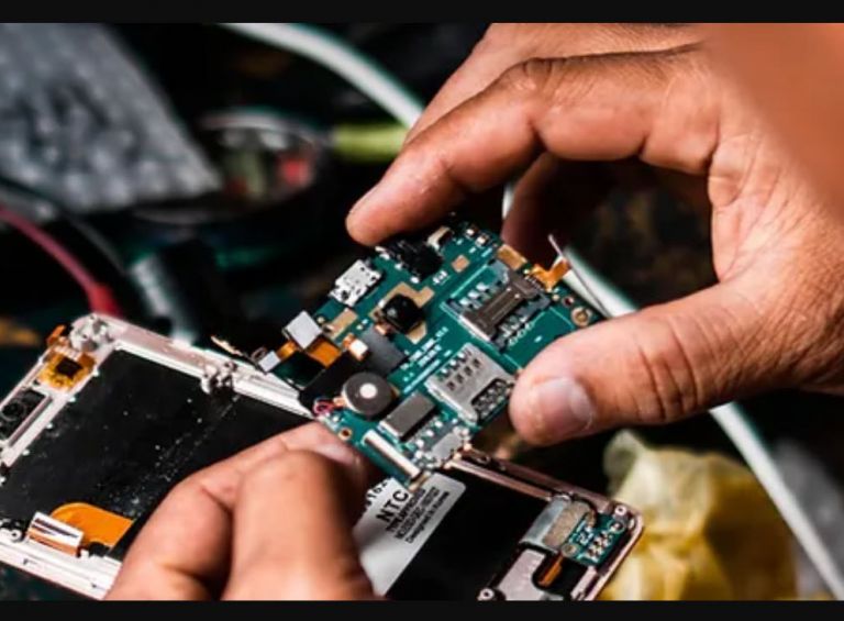
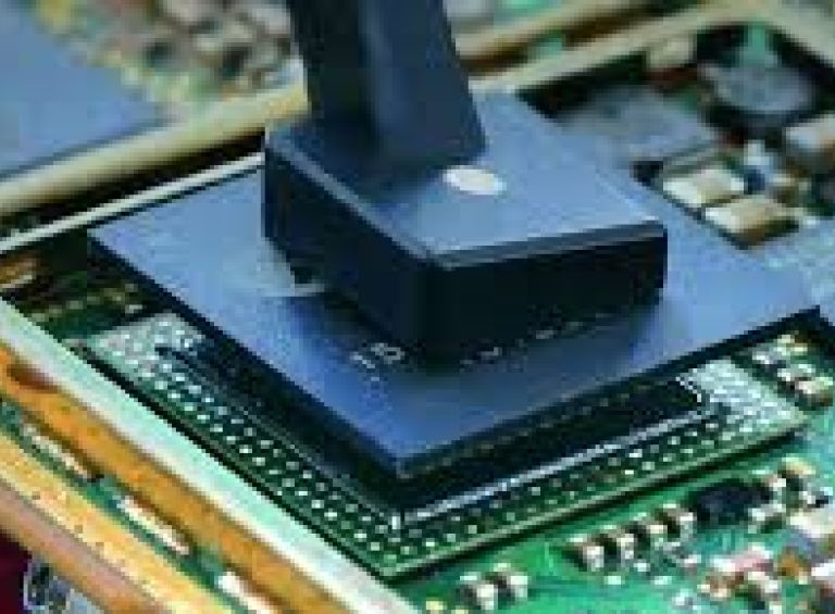
This course focuses on BTC packaging and downstream manufacturing assembly, covering various BTC configurations such as QFN, LGA, MLF, SON, and DFN in both periphery-leaded and solder-ball array packages. By the end of this course, you’ll have the knowledge and practical insights needed to achieve high-yield production and build reliable BTC assemblies in today’s demanding electronics industry.
Taught by a process-driven PCB design engineer with more than 30 years of experience in the electronic and aerospace industry, this three-week program aims to improve the board designs from engineers of varying levels of proficiency and elevate your designs to be more precise and yield-worthy. The principles and methods you’ll learn here are essential for adapting to the specific requirements of all boards, including complex RF and mixed-type designs.

Taught by an IPC-certified industry expert with more than 30 years of experience in the field, this 6-week online program covers the key business and technical concepts that program managers in the electronics industry need to turn customers into lifelong clients.
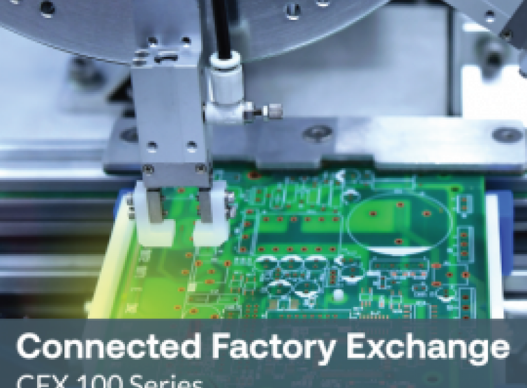
CFX 100 is the first in this 3-part educational series designed to build IPC-CFX expertise. These short, engaging courses provide a comprehensive overview of CFX and machine communication as well as the base requirements for you and your company to get started with CFX. By the end of the series, you will be ready to start sending IPC-CFX messages.

This introductory module provides an overview of CFX and addresses some fundamental questions, including: What exactly is CFX? Who benefits from CFX? and What challenges does CFX address?

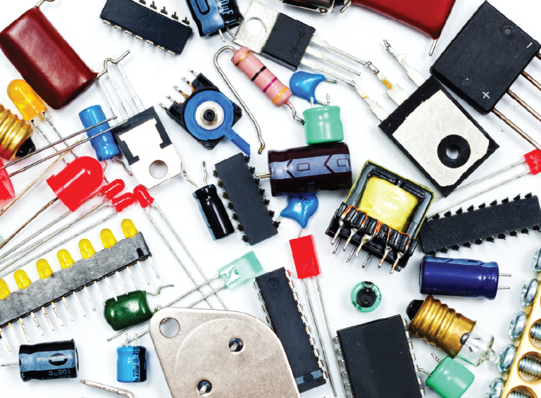
In this course, participants will learn how to identify and determine the value of the most common
electronic components used in PCB assembly, as well as how to use component markings and
assembly documentation to ensure their correct orientation and placement.

In industries where precision and reliability are non-negotiable, from healthcare to automotive, aerospace, and beyond, the presence of counterfeit electronic components can spell disaster. Not only do these components have the potential to cause significant financial loss, but they also pose serious risks to safety and could be life-threatening.
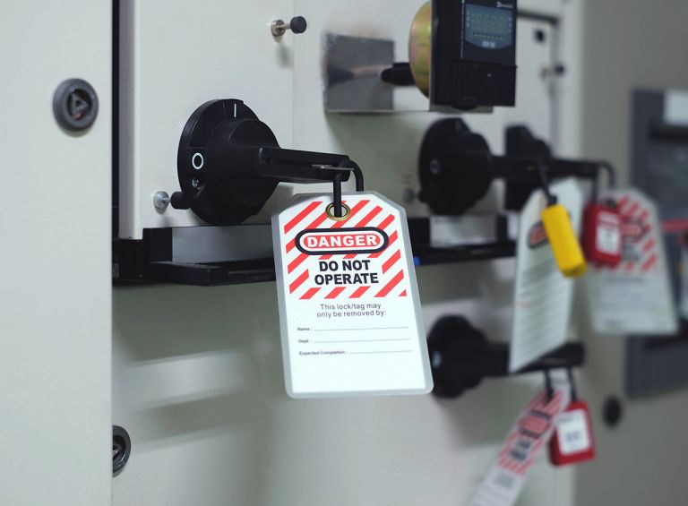
本课程向学员介绍电子制造中最常见的安全实践和工作场所危害。完成本课程后,学员将能够使用旨在确保您和您的同事在制造工厂内安全的关键工具、材料和流程。
能够运用关键工具、材料和工艺流程设计来预防和控制生产场所内的 ESD 影
响。
本课程向参与者介绍 FOD 的成因及在组装车间处理、储存或运输物品时减轻 FOD 影响您可以采
取的步骤。

Engineers make decisions every day that impact manufacturing. Make sure it's a positive impact by introducing the key concepts, tools, materials, and processes critical for engineers to succeed in electronics assembly.

This course introduces the key concepts, tools, materials, and processes that operators need to know to do their best work. Participants can complete the core set of modules to receive their certificate of qualification, then select among nine voluntary modules for process-specific training.

Help your team enhance product reliability, reduce rework and scrap, and ensure customer satisfaction. This comprehensive overview of process control methodology will empower technicians and engineers to utilize the IPC-A-610 Standard and its associated Handbook to consistently meet acceptance criteria throughout the assembly process.
A comprehensive overview of process control methodology including how to utilize the IPC-J-STD-001 Standard and its associated Handbook to consistently conform to acceptance criteria throughout the assembly process.
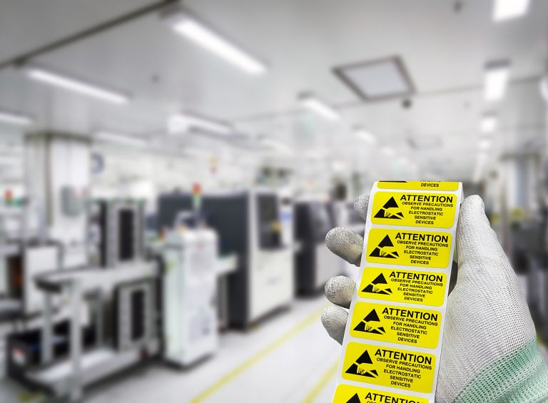
This course introduces participants to the causes of ESD and the steps you can take to mitigate its effects when handling, storing or transporting ESD-sensitive components in a manufacturing facility. These preventive measures and their application are based on ANSI/ESD S20.20 and other relevant standards.
Gain essential skills to design and manufacture high-quality, compliant flexible and rigid-flex printed circuit boards. Led by IPC-certified expert Nick Koop, this interactive two-week course provides a balanced foundation of theory and practical application.
This course introduces participants to the causes of Foreign Object Debris (FOD) and the steps you can take to mitigate its effects when handling, storing, or transporting items in a manufacturing facility. After completing this course, you will be able to employ the key tools, materials, and processes designed to prevent and control the effects of FOD within a manufacturing facility.
This two to four-hour course facilitates mastery of the key concepts required for successful printed circuit board troubleshooting and defect analysis.

Learn how to create industry acceptable solder joints for through-hole and surface mount chip and gull wing components. This innovative multimedia course capitalizes on the power of the hear-see-do methodology to equip students with actionable techniques and best practices they can immediately apply on the job. Students will learn key concepts, tools, and techniques, then use the accompanying practice and project boards, available here, to practice and demonstrate their new skills.
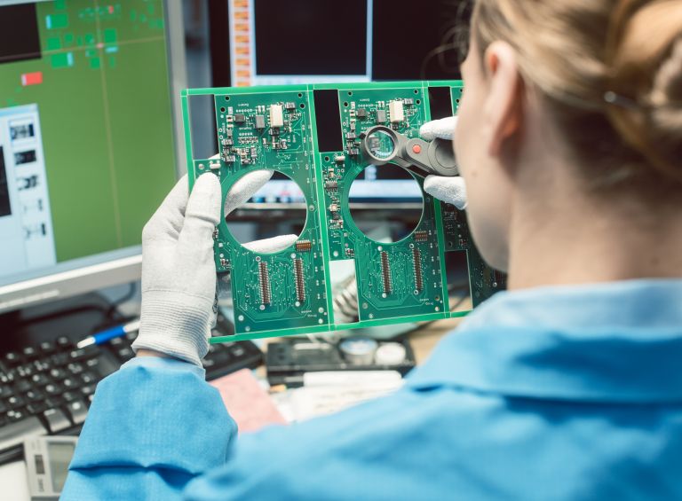
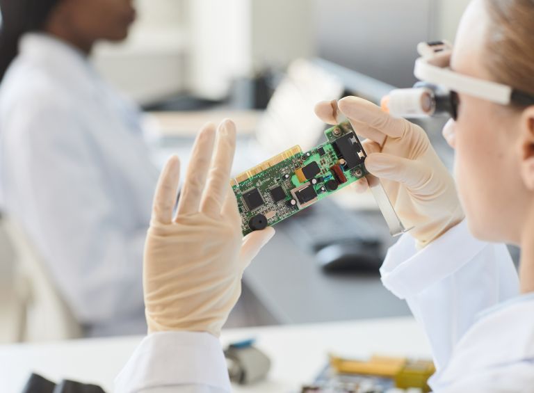
This Inspection of Electronic Assemblies: Introduction course trains participants to perform "incoming inspection" using the essential tools, materials, and processes that deliver consistent quality products. Completion of this course delivers a professional level of proficiency in acceptability standards, inspection methods and tools, documentation, and component characteristics.
This course is ideal for electronics manufacturing professionals who need a foundational understanding of electronic components and the techniques used to ensure their accurate installation on PCB assemblies.
You’ll use IPC-A-610 to align quality expectations, reduce rework, satisfy customer requirements, and support reliable, high-quality production.
You’ll use J-STD-001 to make sound process decisions, align quality expectations across teams, reduce rework, and support consistent, high-reliability outcomes.
This series of ten micro-modules introduces some of the key concepts required to optimize the design of printed circuit boards for manufacture. If you'd like to learn more after completing the series, consider taking the IPC Design for Manufacturability course.

Taught by a certified industry expert with more than 25 years of experience in the field, this 6-week online program introduces participants to the concepts and skills required to create real-world designs that comply with IPC standards. This introductory course will focus on front-end design concepts such as schematic capture, library parts creation, basic electrical engineering concepts, and documentation.
In this course, participants employ the lessons learned in Introduction to PCB Design I to effectively implement their designs using techniques such as multi-layer routing, signal integrity, transmission lines, and more. The course also focuses on how manufacturing and assembly techniques impact design, documentation and manufacturing file generation.
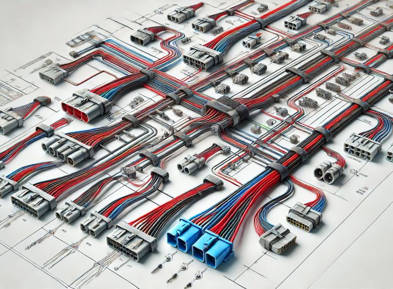
Unleash the potential of wire harness design with our course led by IPC-certified expert Didem Üstün. This two-week intensive program transforms newcomers into skilled designers ready to tackle the complicated challenges of the modern wire harness industry.
In un settore altamente competitivo come quello dell'elettronica, le conoscenze e le competenze di chi progetta il layout del circuito stampato (PCB) e del suo assemblaggio (PBA) hanno un impatto diretto sul successo o sul fallimento del prodotto e incide sul time-to-market. Il corso online sui Fondamenti di PCB IPC è progettato per fornire le competenze necessarie per creare schemi che rispecchino accuratamente l’intento progettuale e la conformità agli standard IPC per la documentazione dello schema.
In un settore altamente competitivo come quello dell'elettronica, le conoscenze e le competenze di chi progetta il layout del circuito stampato (PCB) e del suo assemblaggio (PBA) hanno un impatto diretto sul successo o sul fallimento del prodotto e incide sul time-to-market. Il corso IPC PCB Fundamentals II è pensato per fornire le competenze necessarie alla progettazione di PCB/PBA che rispecchi _ l'intento progettuale, partendo dalle regole di progettazione necessarie e nel rispetto degli standard IPC.
This course is designed to provide designers, assemblers, engineers, and management with a wide overview of PCBA and wire harness manufacturing processes and relevant standards used by industry. Upon completion, participants will be able to:
• Understand the structure and purpose of IPC standards in electronics manufacturing.
• Navigate the IPC standards library and specification tree.
• Identify IPC standards applicable to design, fabrication, assembly, and testing of PCBA and Wire Harnesses.
• Explore the standards covering processes and materials for PCB assembly and testing.
• Create awareness for special industry segments such as automotive and military standards.

Identify the most common IPC standards used by electronics manufacturers, explain product classes and acceptability conditions as outlined in IPC standards, utilize IPC standards to precisely locate specific acceptance criteria, and use figures, illustrations, tables, and units of measurement to assess compliance.
This course provides a practical introduction to the terms, concepts, and acceptability criteria of the IPC/WHMA-A-620 standard as they apply to the role of the operator.
Onboarding manufacturing engineers new to the electronics industry can be a daunting task. What if you had a self-paced course that provides a comprehensive overview of the roles and responsibilities of manufacturing engineers in our industry? IPC worked with industry subject-matter experts and instructional designers to create an introductory course that takes approximately 3-1/2 hours to complete. In addition to understanding the role, participants will also learn to use documentation control systems, product identification, and product traceability.
A comprehensive overview of the stencil printing process for a manufacturing engineer. Participants will learn how to select and store solder pastes & adhesives. They will also learn how to create and maintain stencils, the function of the stencil printer, as well as how to set up the stencil printer for a new product introduction, or NPI, run.

This course provides a comprehensive overview of the surface mount assembly process including information on component considerations, selecting and setting up pick and place machines, and the reflow process. Participants can take this content-specific course to learn more about the role of manufacturing engineers regardless of company size and industry sector.
This course provides a comprehensive overview of component preparation, tool selection, manual component insertion, and automated component insertion in electronics assembly with through-hole components. Participants can take this content-specific course to learn more about the role of manufacturing engineers regardless of company size and industry sector.
In this course, you will be able to set up, monitor, and maintain wave and selective soldering equipment to support consistent, high-quality production. You will know how to apply process parameters, interpret profile data, select the right nozzles and solder pot configuration, and implement maintenance procedures that reduce variation, prevent common defects, and keep your line running efficiently.
The course will start with design of HDI and advanced packaging concepts. This will be followed by embedded component design and the students will see how concepts from HDI are used in the implementation of embedded components. Next, concepts necessary for the design of wearable electronics and how the use of concepts from HDI and Embedded are necessary to achieve the small size and light weight of wearable electronics.
This course introduces advanced PCB design techniques for next-gen applications. Topics include layout, routing, materials, manufacturing, and documentation, with a focus on Ultra HDI, 3D printed electronics, and optical transmission line structures. Learn to design high-performance, manufacturable PCBs for cutting-edge technologies.
This course is designed to provide the skills necessary to effectively implement designs requiring flex and rigid-flex circuits in accordance with product requirements. PCB Design for Flex & Rigid-Flex Boards also focuses on the impact of these designs on manufacturing and assembly techniques, documentation, and manufacturing file generation.

Taught by an industry expert with more than 40 years of experience in the field, this three-week online program is designed to provide the knowledge and skills necessary to reduce or eliminate design, documentation, and capability issues that often arise when completed PCB designs are sent to the fabricator for production.

This course addresses specific design challenges encountered in military and aerospace applications, including the effects of vibration, shock, radiation, and altitude, extended operating temperature range, and other design considerations for high reliability applications. PCB Design for Military & Aerospace Applications also focuses on the impact of these designs on manufacturing and assembly techniques, documentation, and manufacturing file generation.
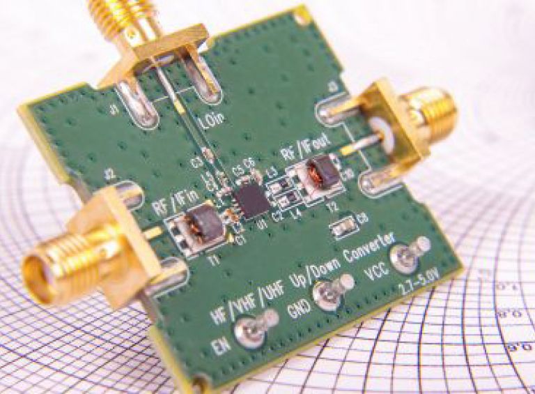
This course provides the theoretical knowledge and practical skills required to create IPC-compliant PCB designs for high-speed analog, radio (RF), and microwave frequencies. This program is designed to provide circuit board designers with a balanced foundation of theoretical knowledge and practical skills in printed circuit board design. Upon completion, participants will be able to:
Design boards for high-speed analog and RF/microwave frequencies.
Understand the trade-offs in materials used in these applications.
Define a board stackup that implements structures that will meet the needs of these designs.
Understand and mitigate signal integrity issues for these designs.
Understand and define the effects of mechanical retention needs for these applications.
Define and implement the tighter manufacturing tolerances needed for these designs.
Understand the use of mixed material stackups in these designs.
Understand the documentation requirements for these designs.

Equip yourself and your team with the knowledge and skills to design and layout PCBs that meet advanced signal integrity requirements, ensuring optimal performance in high-speed digital circuits.
Master the essentials of PCB Fabrication for Operators with a course that guides you step-by-step
through each phase of the process. You’ll gain practical, in-depth knowledge about everything from
inner-layer fabrication and lamination to solder mask application, surface finishes, and final testing

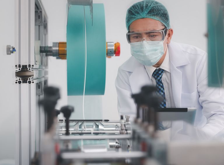
In the competitive printed circuit board fabrication industry, high reliability and high yields are crucial for profitability. That's why process and manufacturing engineers involved in fabrication, assembly, and procurement need to have the necessary knowledge and skills to produce and evaluate top-quality printed circuit boards. This includes understanding materials, chemical processes, equipment parameters, and their impact on board quality.
After completing this course, you will be able to:
Identify and correct control processes that negatively affect circuit board quality
Establish the root cause of potential defects to minimize and prevent loss of quality
Recognize the interrelationships of PCB materials, processes, and equipment and how these relationships affect PCB and PCA quality
Identify the root cause and corrective action for PCB defects, such as interconnect separation, delamination, wedge voids, plating folds, microvoids, surface pitting, and hole wall pull-away
Identify the root cause and corrective action for electrodeposition defects, such as mouse bites, pitting, and domed or crown plating
Identify the root cause and corrective action for solderability and assembly-related issues, such as outgassing, black pad, creep corrosion, and blow holes
Miniaturizing electronics while increasing circuit density and functionality requires advanced
packaging solutions. Among them, Package-on-Package (PoP) is widely used in Integrated Circuit (IC)
design. This course explores PoP packaging and its role in downstream manufacturing assembly,
focusing on high-yield production and product reliability.
Navigate the future of manufacturing design! Dive into the latest DFM trends, from evolving component technology to cutting-edge assembly processes. Master the art of modern manufacturing. Design smarter, today
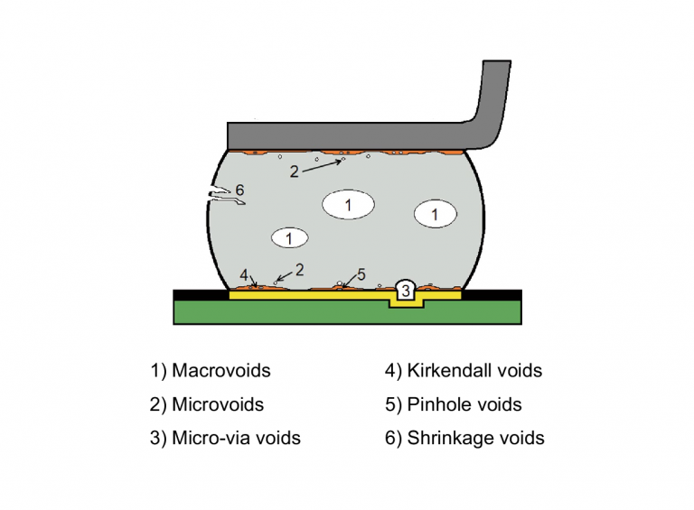
This course aims to enhance product reliability and maintain high production yields by offering comprehensive insights into solder joint voids. We will explore the origins of these voids, understand their causes, and analyze their impacts on solder joint efficacy and overall product dependability.
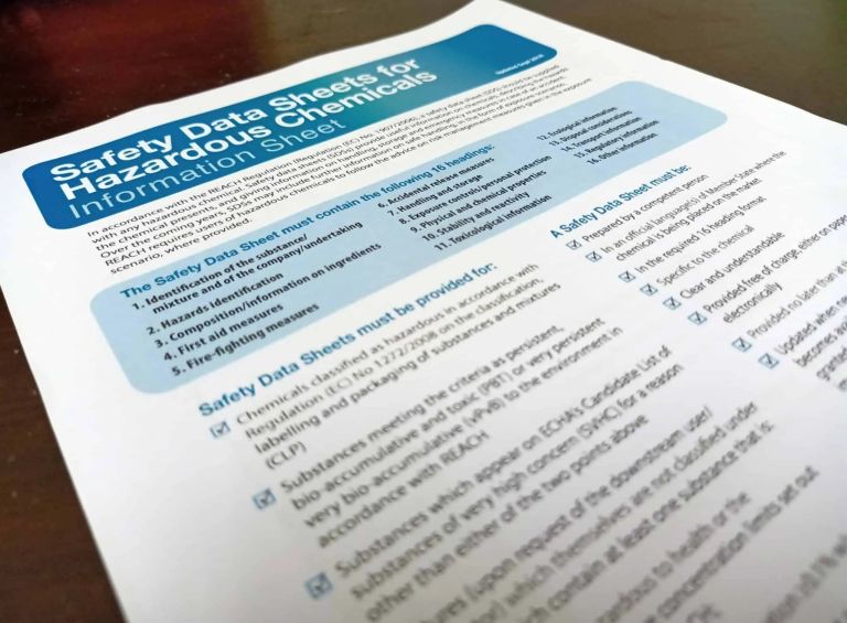
In electronics manufacturing, chemicals are everywhere, from cleaning agents to conformal coatings, and mishandling them can risk health, safety, and production. This course equips engineers with the skills to read, interpret, and apply Safety Data Sheets (SDS) to make informed decisions that keep people safe and processes compliant.
This course is ideal for operators, technicians, supervisory personnel and other staff members that must consistently and effectively employ the key tools, materials, and processes designed to keep workers safe within a manufacturing facility.

Learn how to mitigate the health and safety risks associated with soldering. The course covers various topics, including the hazards related to soldering tools and materials, implementing effective safety measures, and maintaining a safe soldering environment.
Dive into the dynamic world of semiconductor chips with our expertly designed course, crafted for professionals who aim to master the industry's intricacies. From concept to creation, explore each stage of the semiconductor lifecycle — design, manufacturing, assembly, and testing.
Understand the foundational principles of electrical systems and electronic hardware. Topics include basic DC and AC electrical theory, passive and semiconductor components, the use of basic test tools, and familiarity with common methods of inspection.

The Train-the-Trainer course equips subject-matter experts (engineers, technicians, CITs/MITs) with the instructional knowledge, pedagogical and andragogical principles, and facilitation skills necessary to effectively teach operators, technicians, and engineers in electronics manufacturing.
The Transform Your Constraint Engineering PCB Designs course is developed to provide specific paths to understanding Electrical and Mechanical Models which allows the experienced PCB design engineer opportunities to generate specific routing features to help improve, develop, and advance their design skills into a robust engineering skill set.
Equip your team to quickly and effectively identify, analyze, and address PCBA production defects. Jim Hall and Phil Zarrow, the authors of Troubleshooting for Electronics Manufacturing and the acclaimed BoardTalk podcast, offer decades of practical insights that students can immediately use to increase reliability, yields, and cost savings.

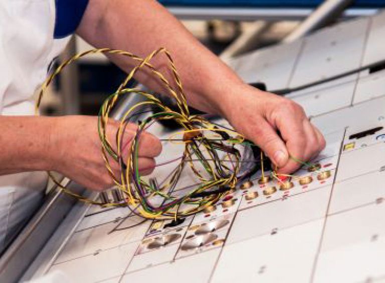
Learn a specific set of knowledge and skills that every operator needs to build quality wires and cable harnesses all contained in as little as 16 hours of training.